Image Credit: e_rik/Shutterstock.com
A novel fabrication method and liquid metal gallium could help form new 2D superconductor technology and boost transistors.
The number of transistors in integrated circuits (IC) — a set of electronic circuits on one small flat piece of semiconductor material, typically silicon — doubles every few years. However, this generalization has started to fail, with transistors now becoming so small that shrinking them any further is a task that pushes the limits of silicon-based technology too far.
There is a glimmer of hope, however, provided by the use of ultra-thin two-dimensional semiconductors. Yet, such devices are not perfected. One of the problems that hamper this technology is the appearance of grain boundaries in 2D semiconductors when upscaled. This flaw can seriously hamper charge carriers reducing the efficiency of such semiconductors.
Researchers at the School of Chemical Engineering, University of New South Wales (UNSW) have developed a method of using liquid gallium to perfect 2D semiconductors made from molybdenum disulfide (MoS2) — potentially solving this issue.
The team’s research is published in the latest edition of the journalAdvanced Functional Materials.
Two-dimensional semiconductors are so thin that they allow free charge carriers — namely electrons and pseudo-particle ‘holes’ in transistors — to propagate unimpeded carrying information across their ultra-thin plane.
Confining these charge carriers allows easy semiconductor switching and creates directional pathways for the charge carriers. This allows them to travel without scattering, resulting in an infinitely small resistance for the transistors, saving energy.
Therefore, in theory, 2D semiconductors can create transistors that do not waste energy during on/off switching. These transistors could be switched between states quickly and achieve a state of zero resistance while non-operational. This can occur if the technological barriers opposing such devices can be torn down or navigated around. That is where liquid gallium comes in.
Using Gallium to Smooth Out Semiconductors
Molybdenum disulfide (MoS2) has been intensely investigated as a material ideal for constructing 2D semiconductors, but the substance comes with a particular characteristic limiting its use. Despite having interesting and useful electronic capabilities, when MoS2 is shaped into large 2D sheets, significant grain boundaries develop. These boundaries cause charge carriers to bounce off them, disturbing the flow and increasing resistive loss.
Current large-scale deposition methods are not capable of creating grain-boundary-free MoS2 needed to make ICs. The researchers from UNSW believe that liquid gallium and a new deposition method could solve this problem.
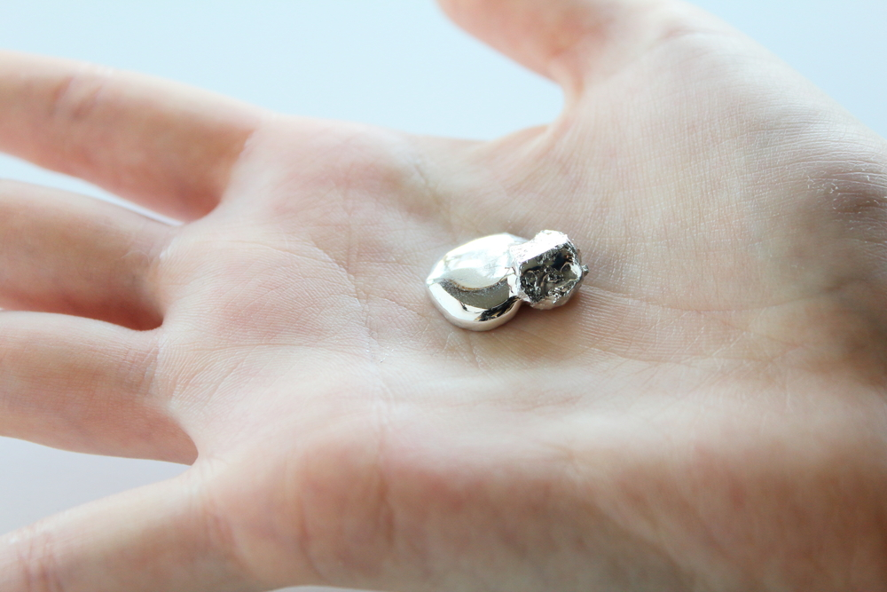
Gallum is an extraordinary metal that possesses a uniquely low-melting-point of just 29.8 °C. This means that while it is solid at room temperature, gallium can easily be turned into a liquid when placed in your hand. Being a melted metal, the surface of gallium is atomically smooth, while the fact that it is a metal in conventional terms means that its surface also has an abundance of free electrons.
The researchers achieved grain boundary-free MoS2 by placing the molybdenum and sulfur sources in proximity to the gallium's surface while it is in its liquid state. This ‘imprints’ the 2D material on the atomically smooth surface of the gallium.
Already naturally nucleated and grain boundary-free due to this first step, the MoS2 then undergoes a heat treatment process that changes the material’s characteristics to increase ductility and reduce the hardness to make it more workable, called annealing. This second step enables the team to scale-up MoS2 production. The result is a large area MoS2 structure with no grain boundaries.
The team — led by Professor Kourosh Kalantar-Zadeh of UNSW — believes that the process is an important step in creating ultra-smooth semiconductors. The next step for the researchers will be to expand their methods and create other 2D semiconductors and dielectric materials that can also be utilized in transistors.
What semiconductor metrology tools are available on the market today?
References and Further Reading
Kalantar-Zadeh. K., Kaner. R. B., Daeneke. T.,et al.(2020) Self-Deposition of 2D Molybdenum Sulfides on Liquid Metals.Advanced Functional Materials,https://doi.org/10.1002/adfm.202005866
Disclaimer: The views expressed here are those of the author expressed in their private capacity and do not necessarily represent the views of AZoM.com Limited T/A AZoNetwork the owner and operator of this website. This disclaimer forms part of theTerms and conditionsof use of this website.