Jun 11 2015
Mirtec,“检查技术的全球领导者”将在Semicon West 2015展示其最新的包装系统解决方案(SIP)检查和测量;2015年7月14日至16日,在加利福尼亚州旧金山的莫斯汀中心。邀请访问者参加#2343展位,以详细展示这项令人兴奋的新技术。

MITEC北美销售和服务部的Brian D'Amico总裁说;“对小型化的需求不断增长,生产成本降低的功能越来越高,导致包装(SIP)解决方案中系统的行业需求。SIP是单个软件包中包含的许多集成电路。SIP执行电子系统的所有或大多数功能。
These packages are typically used in mobile devices such as cell phones and digital music players. Dies containing integrated circuits may be stacked vertically on a substrate and are internally connected by wire bond to the package. Alternatively, with a flip chip technology, solder bumps are used to join stacked chips together. As one can imagine, this complex arrangement of advanced packaging presents a challenge to the inspection environment.”
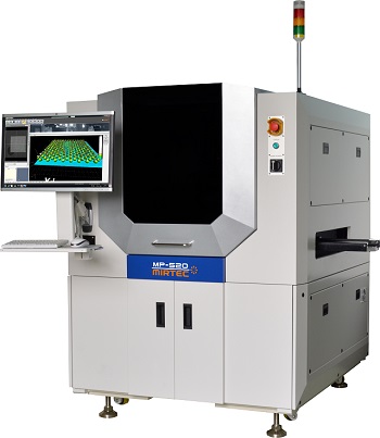
MIRTEC的MP-520系统专门针对与SIP检查有关的挑战。The MP-520 combines Precision Linear Drive Motor Technology with MIRTEC’s exclusive 25 Mega Pixel CoaXPress Camera System, a 3D Confocal Measurement system and revolutionary OMNI-VISION 3D Digital Multi-Frequency Moiré Technology to provide high-speed, high-resolution inspection and measurement for SiP and other semiconductor applications. The MP-520 also is configured with eight (8) phase color lighting and four (4) 10 Mega Pixel side-view cameras.
MP-520适用于测量和检查以下制造标准:
- Solder Ball/Bump – Presence, Pitch, Offset, Height, Co-Planarity and Bridging
- Bond Wire - Short, Broken, Shift and Loop Height
- Chip Bond - Offset, Height, Crack and Chip
- 离散设备 - 存在,偏移,高度,共同计划和焊料圆角
- 散热器 - 存在,偏移和高度
- Under-Fill – Presence, Fillet and Height
- PCB - Scratch, Contamination and Bridging
- Package - Warpage, Crack, Marking, Dimensions and Chipping
Inspection and measurement results are stored in a central database, enabling customers to remotely access SPC data through MIRTEC’s INTELLISYS total quality management system software. This software suite promotes continuous process improvement by allowing the manufacturers to track and eliminate defects on inspected assemblies.
INTELLISYS also provides remote debugging and monitoring of up to eight production lines, allowing MIRTEC customers to further maximize the efficiency of the inspection process.
“Mirtec通过为制造环境提供前所未有的绩效,质量和成本效益,在半导体检查行业中享有良好的声誉,”continued D’Amico,“我们为我们的高级后端检查解决方案的越来越多的全球半导体公司实现了高水平的客户满意度。我们期待在为期三天的活动期间欢迎游客参加我们的展位#2343。”